
Product Portfolio
Welcome to our Product Portfolio section.
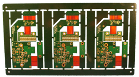
A list and typical photos of PCBs made by Alpha Circuit Corporation is displayed in the following section of this page. An assortment of PCBs is shown below:
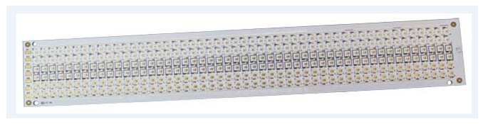
PCB w/ Heat Sinks & Thermal Management
We have an extensive R&D portfolio and experience in making PCBs that need effective thermal management for a variety of RF analog or digital or hybrid circuits. We formulate and tailor the thermal interface material compositionally to meet specific requirements of the customer in terms of thermal, mechanical and environmental stability of the overall electronics device and module, and offer design guidelines to meet specific application criteria.
PCB for RF and Microwave Applications
Antenna design and RF layout are critical in a wireless system that transmits and receives electromagnetic radiation. The PCBs made for RF or microwave applications require proper laminate material selection. These laminates are advanced composites with very specific characteristics for dielectric constant, loss tangent, and co-efficient of thermal expansion (CTE).
For example, the wireless range that an end-customer gets out of an RF product with a current-limited power source depends greatly on the antenna design, the enclosure, and a proper PCB layout and fabrication criteria. For a PCB made for RF or microwave telecommunication application it is important to have general layout considerations for RF trace, power supply de
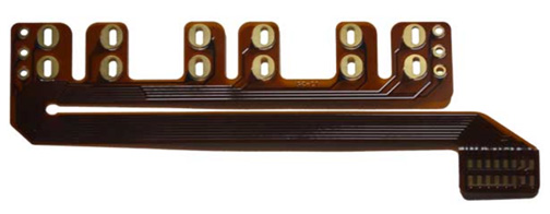
Flexible Circuits
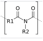
In their simplest form, flexible circuits are PCBs made of materials that allow for a non-planar positioning within the end product. Typical materials are basically mostly polyimide-based, and can go under trade names such as Kapton (DuPont). Polyimide is a polymer of imide monomers:
Due to their high temperature resistance and robustness, they have been enjoying diverse commercial applications in flexible PCBs most notably in display electronics in a variety of industries such as automotive, aerospace, portable electronics, medical, and LEDs.
Applications for Flex Circuits
Often flexible circuits are used for applications that have repeated flex cycles, such as cellular phones, doors, etc. A growing application for flexible circuits is their use as a connector in LED-based lighting systems. Often, there are two components: a metal substrate LED PCB; an FR-4 based digital driver PCB. These two devices are often connected with a high profile and sometimes costly connector cables. Using a flexible PCB in its place can offer a lower profile, slimmer design, and higher reliability.
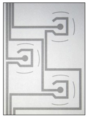
Blind Vias start on an outer layer but terminate on an inner layer; Buried Vias exist only between inner layers and do not begin or terminate on an outer layer. Another variant of these technologies is stacked vias. Stacked vias are used when a blind via is required but exceeds an aspect ratio of 1:1 and cannot be formed through sequential lamination due to another blind or buried via beginning on the same layer as the blind via's termination layer.
Applications
Blind, buried, and stacked vias are used to save PCB real estate. Also, some of today's tight componentry requires blind vias to be used in order to properly fan out the internal traces of the component on various layers of the PCB.
PCB With Controlled Impedance
As the speed of signal switching on a PCB increases, the electrical properties of the traces carrying signals between devices become increasingly important. The impedance of a PCB trace is controlled by its configuration, dimensions (trace width and thickness and height of the dielectric laminate), and dielectric constant of the laminate. It is important to have a controlled impedance of various traces that are connecting active and passive components. A tightly controlled impedance matching of these traces ensures that the propagating signals do not result in any losses, part of the signal reflected and only a part transmitted. These reflections are likely to cause aberrations on the signal which may degrade circuit performance such as noises and low gain.
It is important that the customer specifies the impedance values and tolerances for the board to be fabricated by us. Alpha provides solutions for design and final product verification and any other questions the customer may have.
Standard impedance tolerances are within 10%. However, our engineering team routinely produces Controlled Impedance PCBs to hold 5% impedance tolerance. We are able to achieve this by maintaining a database of past stack-up and resulting thicknesses that allow our front-end engineers to run tight impedance calculations. Further, numerous in-process checks are made to ensure that fabrication results are as close to the designed values as possible.
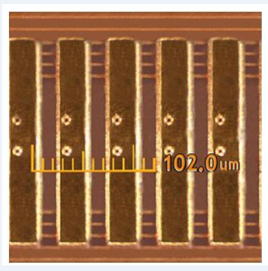
High Density Interconnect (HDI) PCB w/ Blind/Buried stacked vias
High Density Interconnect
PCB WITH EMBEDDED COMPONENTS
Typically embedded components include embedded resistance and embedded capacitance. These passive components can occupy a great deal of the surface real estate of a PCB. By embedding these to internal layers, not only can PCB sizes be reduced, but many cost increases are offset by higher production throughput making this a win-win situation for the PCB user.
Embedded Resistance
Our experience with embedded resistance has been primarily with materials from Ticer Corporation (www.ticertechnologies.com). Their embedded resistance material can be procured on a variety of materials, including from suppliers Rogers and DuPont. It's fairly easy to work with, making achieving discrete resistance values easier to achieve in consistency.
Embedded Capacitance
We've produced PCBs with embedded capacitance using 3M's C1012 rigid substrate and DuPont's Interra flexible substrates. The challenge in manufacturing with these materials is that often, due to their thin properties (down to 0.5 mils), they are difficult to process through conventional equipment, making a flexible PCB supplier the ideal choice for producing this technology.
Printed Electronic PCB
This is an emerging technology in the PCB manufacturing. The circuit is made by an additive process instead of using the conventional subtractive route wherein the circuit is etched out after photoresist lamination, lithography, and so on as shown in the Process Flow Diagram
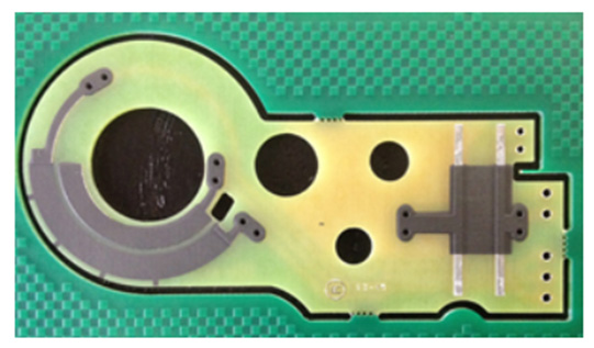
Carbon Ink PCB
Carbon ink is typically used to create a protective contact surface for switches. It is much more cost effective than hard electroplated gold. The morphology, high robustness and wear and tear resistance of carbon ink make it a very attractive candidate for potentiometer slider applications.
This PCB is typically 2-layer rigid board with a copper thickness of 1 to 2 ounce and final surface finish of RoHS tin or HASL. PCBs with carbon ink deposit with 110 ohm for resistor application and 5,500 Ohm resistance for potentiometer application are typical examples.
Edge Plating Castellation
Description coming soon. Thanks for your understanding and interest in Alpha Circuit